
The new 3D AOI uses a simple yet extremely effective and repeatable technology called Multi-Frequency Quad Moiré lighting (Figure 1) to make measurements of all the components on the PCB. It works by projecting a line pattern at a given angle then shifting and varying the patterns frequency for a total of 8 different unique patterns (Figure 2). To accomplish this the Mirtec uses four opposing pattern projectors that are positioned at 0, 90, 180 and 270°. The result is a total of 32 images for the 3D computation as well as an additional 7 images with standard 2D imaging from the main camera.
These line patterns are captured by the
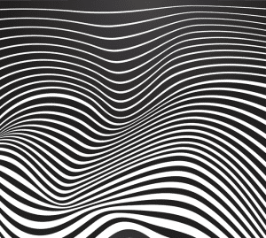
M oiré pattern on a curved surface
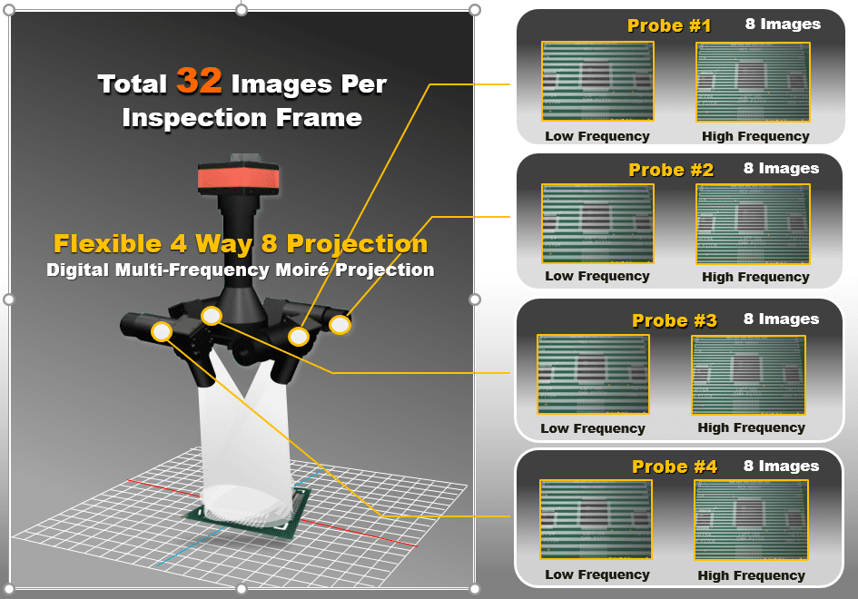
Multi-Frequency Moiré Projectors
The primary advantage of a 3D AOI over traditional 2D AOI is the ability to give a true measurement of components. With these measurements, you can establish criteria/tolerances for the length, width, height, coplanarity, lead height as well as solder filet height, angles and volume. This adds an ever-increasing number of variables that can be inspected. For instance, let’s consider a standard 1206 ceramic capacitor. A typical 2D AOI compares the component being inspected to an image or series of images of a good component that is stored in the AOI machine’s library. This comparison has some drawbacks as it is subject to a higher rate of false calls and escapes. For instance, if the component varies in size, shape, or color slightly and there is not a good representation of this in the good image library then the component will be flagged as a defect. Consider also how many shades of tan there are for the ceramic material of the capacitor. It is common to have several shades from one
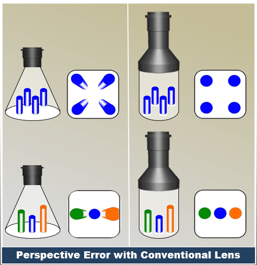
Conventional lens (left),
Telecentric lens (right)
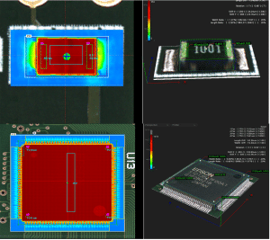
3D inspection of SMT components
Where 3D AOI shines is that ability to measure all the features on the component and compare them to the present criterion in the machines database. The machine can then rely on measurements instead of comparing 2D images. Furthermore, with 3D AOI you can measure the capacitors placement position (X, Y
In conclusion the current 3D AOI technology allows Altek Electronics to better automate inspection of PCB’s in regards to surface mount technologies to distinguish what is really bad from good while offering improved coverage, capability and improved throughput. ?