Employees eager to learn new skills, adding to their qualifications. Way to go
Thanks to our trainer David for his expertise and guidance.
Employees eager to learn new skills, adding to their qualifications. Way to go Stephen, Valerie, Ted, and Maria!
Employees eager to learn new skills, adding to their qualifications. Way to go
Thanks to our trainer David for his expertise and guidance.
Attendees will see examples on both the manufacturing floor as well as administrative functions where teams are improving safety and efficiency through formal workplace organization
Attendees will see examples on both the manufacturing floor as well as administrative functions where teams are improving safety and efficiency through formal workplace organization, identifying waste through process mapping, improving communication through visual management, improving flow through kaizen, reducing set up times through set up reduction activities, and addressing gaps through root cause problem-solving.
Agenda: 8:30 a.m. Registration, networking and continental breakfast
9:00 a.m. Presentation on LEAN/Continuous Improvement at Altek
9:45 a.m. Factory Tour – examples of LEAN and Continuous Improvement initiatives
11:00 a.m. Depart
Price: SMTA member: $25 Non-member: $35
TORRINGTON — Made in Connecticut was the theme on Wednesday when 5th District Democratic candidate Mary Glassman toured Altek Electronics Inc. at 89 Commercial Blvd.
“I want to help facilitate new jobs,” Glassman said during the tour.
She noted that 13,000 jobs in Connecticut go unfilled because potential workers do not have the skills required for manufacturing jobs.
“There are good jobs, good pay and good futures,” in industry, Glassman said.
She pointed to a a success story from Torrington High School’s Innovation Class, which collaborates with Northwestern Connecticut Community College. Through the program, Altek employee Alain Malcom learned the skill of soldering and was hired two years ago. The 20-year-old now works as a junior buyer.
That type of collaboration could boost the economic health of the 41 towns within the sprawling 5th district.
“I know how cities make decisions,” said Glassman, who served as Simsbury’s first selectwoman for 16 years. “We can leverage state and local government.”
Ravi Kailan, director of operations for Altek, said the company grew by 15 percent about a year ago. Through the application of lean engineering, which practitioners use to pinpoint more effective manufacturing processes, Kailan said Altek was able to recoup the cost of a $365,000 machine in less than two years.
Luciana Rodriguez, a trainer for the surface mount team, said she’s learned how to help her team be more efficient.
“What used to take two days now takes less than a day,” she said.
That result allows the company to grow its business, Kailan added.
Altek, a family-owned company with almost 200 employees, opened in 1972. Sabrina Beck, vice president and co-owner of the company, said Mexico and China are their biggest competitors. “We are constantly asked to reduce prices,” she said.
“I want to keep the cost of working in Connecticut down,” Glassman responded.
Glassman’s Democrat opponent for the 5th District seat is Jahana Hayes, of Wolcott. She is a Waterbury teacher who was named national teacher of the year in 2016.
They will face off in the primary election on Aug. 14.
A veteran-owned small business privately held by three family members (Stephan Altschuler, David Altschuler, and Sabrina Altschuler Beck), Altek Electronics, Inc. manufacturers printed circuit board assemblies and box builds for many industries including medical, military, industrial and telecommunications.
When Altek Electronics Inc. CEO David Altschuler talks about understanding the company’s customers, he means he visits the customer’s plant once a week, walks through security wearing the badge they gave him 18 years ago, and he talks to various people in the receiving department, production, engineering, and supply chain about what they need and how Altek is performing.
The latest and greatest equipment along with the people who are passionate about what they can do for you.
This investment aids in our goal of continuously improving and staying at the leading edge of available technologies in the field of electronic assembly. We believe this gives our customers best in class value on products and services.
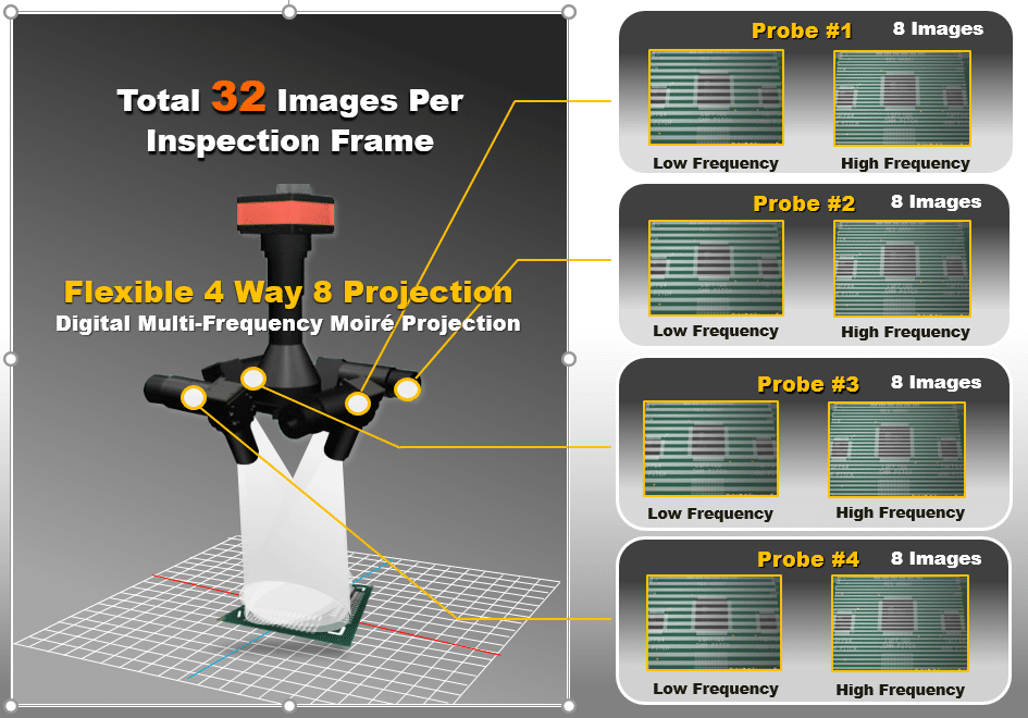
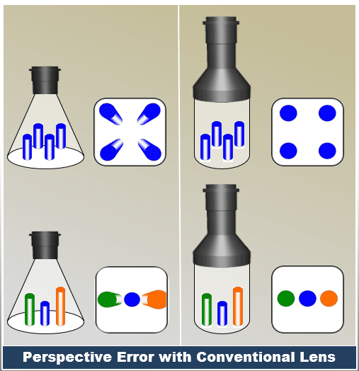
The new 3D AOI uses a simple yet extremely effective and repeatable technology called Multi-Frequency Quad Moiré lighting (Figure 1) to make measurements of all the components on the PCB. It works by projecting a line pattern at a given angle then shifting and varying the patterns frequency for a total of 8 different unique patterns (Figure 2). To accomplish this the Mirtec uses four opposing pattern projectors that are positioned at 0, 90, 180 and 270°. The result is a total of 32 images for the 3D computation as well as an additional 7 images with standard 2D imaging from the main camera.
These line patterns are captured by the

The primary advantage of a 3D AOI over traditional 2D AOI is the ability to give a true measurement of components. With these measurements, you can establish criteria/tolerances for the length, width, height, coplanarity, lead height as well as solder filet height, angles and volume. This adds an ever-increasing number of variables that can be inspected. For instance, let’s consider a standard 1206 ceramic capacitor. A typical 2D AOI compares the component being inspected to an image or series of images of a good component that is stored in the AOI machine’s library. This comparison has some drawbacks as it is subject to a higher rate of false calls and escapes. For instance, if the component varies in size, shape, or color slightly and there is not a good representation of this in the good image library then the component will be flagged as a defect. Consider also how many shades of tan there are for the ceramic material of the capacitor. It is common to have several shades from one
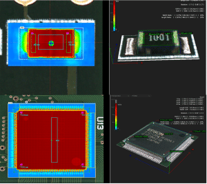
Where 3D AOI shines is that ability to measure all the features on the component and compare them to the present criterion in the machines database. The machine can then rely on measurements instead of comparing 2D images. Furthermore, with 3D AOI you can measure the capacitors placement position (X, Y
In conclusion the current 3D AOI technology allows Altek Electronics to better automate inspection of PCB’s in regards to surface mount technologies to distinguish what is really bad from good while offering improved coverage, capability and improved throughput. ?
Altek employees consumed 13,000 K-Cups of coffee last year. After learning about the negative impact plastic K-Cups have on the environment, Altek managers worked to find a greener solution. We switched to biodegradable coffee pods, which are more environmentally friendly and cost less, saving over $3,000 per year.
Here are employees Luis Martinez and Elizabeth Reyes in front of the new coffee pod vending machine. Offering 12 different flavors in a sustainable, fresher tasting cup makes Altek a friendlier place to work.
In May 2017 Altek made an advancement in PCB cleaning, rinsing, and drying that’s similar to switching from just brushing the surface of your teeth to brushing and flossing in between the tight spaces of the teeth.
Is brushing all you need to do to clean and protect your teeth and gums? No. Just like batch technology is no longer enough to clean your printed circuit boards.
Brushing your teeth removes plaque buildup from the front and back surfaces of teeth. But to fully clean and protect teeth you need to floss so you remove plaque from between teeth and underneath your gums. In May 2017 Altek made an advancement in PCB cleaning, rinsing, and drying that’s similar to switching from just brushing the surface of your teeth to brushing and flossing in between the tight spaces of the teeth.
As of May, 2017 Altek has the capability of cleaning, rinsing, and drying PCBs with the latest inline technology. From the Technical Devices Company, Altek purchased a Nu/Clean 800 Series inline aqueous cleaner.
Throughout the PCB industry, assemblers face a daunting and growing challenge. Today’s PCBs feature much greater density, complexity, and miniaturization. Tomorrow’s PCBs will be even harder to clean. The narrowing space between components and boards makes thoroughly cleaning them increasingly difficult. Board assemblers who currently clean with a batch-type cleaner are looking for solutions to increase cleaning capability. Altek has found the solution.
The Altek plant now features a three foot wide, 25 foot long industrial “washing machine.” A main feature of this Nu/Clean machine is its flood box technology.
The machine’s flood box technology involves a “bathtub” with water jets that soak the boards and agitate the flux residues to clean underneath low standoff components. The circuit boards are submerged completely, so no area is missed. Because the boards are neither lowered nor raised there’s no jarring or potential to dislodge or damage components on the conveyor. A trip through the flood box combines a pressurized spray from nozzles with a flood of turbulent fluid. The next step is conventional top and bottom spray bars. Along with the rinsing and drying features, these cleaning features provide at least five major benefits to Altek clients.
Industry research finds that this type of inline aqueous cleaning provides greater penetration of low clearances within the electronic assembly. The new equipment technology is effective at cleaning both flux residues and ionic contamination under the body of the component. The soaking action of the cleaning agent on the surface of the printed circuit board softens the flux residue. When that residue gets bombarded with the pressurized spray, the residue floats free from the PCB. And because the cleaning agent pools onto the board, it lowers surface tension, helping to penetrate under tightly spaced components.
Another key feature—reduced coherent spray jets—provides protection against dislodging labels, removing part marking, or negatively impacting board components. Coherent spray jets deliver the cleaning agent at higher pressures onto the printed circuit board. The pressurized spray jets provide strong deflective forces for penetrating and moving the cleaning agent under the component. But having too many spray jets or too strong of a stream can undercut labels, remove part marking, and potentially affect other material compatibility effects. The Nu/Clean 800 at Altek uses fan sprays that reduce the impact to the electronic board. Fifteen stainless steel pumps give just the right balance of pressure and flow to remove residues and contaminants.
The cleaning agent in the new equipment is attracted to water. With a layer of water covering the surface of each board within the rinse section, removal of the cleaning agent under bottom termination components is improved.
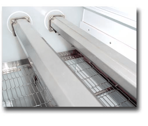
The double air curtain and anti-drag out zone is one of many features that reduces cost by saving chemicals
This new cleaning technology provides Altek with higher throughput. We can now clean more boards at a faster pace, enabling us to meet customers’ tight schedules. The reduction in human touch means there are fewer opportunities to introduce defects through human error.
Altek produces more than 500 different products for customers. The Nu/Clean has the flexibility to handle a wide variety of these products. And, to meet customer requirements, we can adjust many factors including temperature, conveyor speed, and pump pressure. Our first test run on May 2 demonstrated how this new technology will advance the cleanliness and effectiveness of customer’s circuit boards.
Your dentist knows a healthy mouth is a portal to a healthy body. Altek knows a great system for cleaning, rinsing, and drying circuit boards is a portal to delivering high performing, high quality PCBs.
David Altschuler was recently promoted to the position of CEO and will be leading many initiatives to maintain our strength in LEAN, quality and on-time delivery. David started his career at Altek in 1992 and has held several key positions including leading administration, IT, materials, and customer service. In 2003 David was promoted to the position of Vice President of Finance and Administration. David played a key role in facilitating the company’s move to our current location, and he’s been managing one of our largest customers for nearly two decades.
To fill the position made available by David’s promotion, Kevin Bair was selected as Altek’s new Director of Finance & Administration. With extensive experience in electronics manufacturing and finance, Kevin comes to Altek from Winchester Electronics where his managerial role focused on finance, accounting, and production support in several locations around the world.
We are excited to introduce Ravi Kailan as Altek’s new Operations Manager who is responsible for all activities related to manufacturing. Ravi, a six-sigma black belt, joins Altek with a strong background in operational management, most recently from a senior operations role at DRS Consolidated Controls.
Together Altek’s management team and our employees and will work hard to maintain the trust we’ve established with our customers and continue to make a positive impact in 2017.